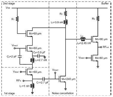
In this work, common source Low Noise Amplifier using inductively degenerated technique is designed to meet Radio Frequency (RF) range 2.45 GHz-2.85 GHz. The designed LNA is implemented using single and multi-finger transistor logic. The transistor geometry greater than 300 μm has been split into multiple fingers using multi-finger technology. The schematic is captured using ADS. The performance of LNA for various technologies has been analysed using PTM 180 nm, PTM 130 nm and PTM 90 nm models. The amplifier with single transistor achieves minimum noise figure of 0.178 dB noise figure and maximum gain of 20.045 dB using 130 nm model technologies for Bluetooth applications. Similarly the minimum noise figure of 0.288 dB and peak gain of 17.971 dB is obtained using multi-finger MOSFET of PTM 90 nm technology.


